
Quantum wells
 المؤلف:
Peter Atkins, Tina Overton, Jonathan Rourke, Mark Weller, and Fraser Armstrong
المؤلف:
Peter Atkins, Tina Overton, Jonathan Rourke, Mark Weller, and Fraser Armstrong
 المصدر:
Shriver and Atkins Inorganic Chemistry ,5th E
المصدر:
Shriver and Atkins Inorganic Chemistry ,5th E
 الجزء والصفحة:
673
الجزء والصفحة:
673
 2025-10-14
 285
285
Quantum wells
Key points: Quantum wells consist of a thin small band-gap material sandwiched between thick layers of large-gap materials; multiple quantum wells can enhance the effects of quantum wells when the wells do not interact. A quantum well is typically composed of two semiconductor materials with different band gaps, such as Al1-xGaxAs and GaAs. The smaller band-gap material (GaAs) is sandwiched between layers of the larger band-gap material (Al1-xGaxAs), and the thickness of the layer of the small band-gap material is confined to the nanometre scale (Fig. 25.21). Electrons are confined in the layer of the small band-gap material along the growth direction; the barrier height is the difference in the energy levels of the band edges for the two materials. Therefore, the energy states in the smaller gap material are quantized along the growth direction, similar to the quantization of energy in a QD. The electronic wave functions are spatially extended in the direction parallel to the layer and therefore the energy levels are not quantized. As for a QD, the optical properties of quantum wells can be tailored and both interband (Between the valence and conduction band) and intraband (between the quantized sub-bands) absorption and emission can be controlled. Both In1-xGaxAs/GaAs and Al1-xGaxAs/GaAs quantum wells have been widely studied, and the optical transition has been observed to move to higher energies compared to the bulk when the thickness drops down to about 20 nm. The main use of quantum wells is in semiconductor lasers, where the small-gap quantum well is the active layer in the device. Typical QW lasers use the interband transitions, but intraband lasers are also being developed and are discussed below. Many of the effects that occur in quantum wells can be enhanced by using superlattice structures, the periodic repetition of quantum wells along the special direction (the z-axis). In the context of semiconductors these superlattices are called multiple quantum well (MQW) structures. If the active layers (the small band-gap layers) do not interact, then the electrons are confined to a given layer and are unable to tunnel between them. The use of MQW structures in this case increases the absorption or emission from a given device, as there are multiple levels. For example, an MQW laser has much higher power output than the corresponding single quantum-well laser. If the wide band-gap layers are thin enough, one QW interacts with the adjacent QW and electrons can tunnel between them. This phenomenon is used in quantum cascade (QC) lasers, which operate at high powers in the IR region. The laser characteristics of these materials are fundamentally different from those of semiconductor diodes and MQW lasers in a variety of ways. In a QC laser, only one type of carrier (electrons) is necessary to achieve laser action; in the other two, both electrons and holes are required. In addition, in the QC laser, the transitions are intraband transitions that arise from the quantization of the valence band. The QC lasers are constructed from 13/15 (III/V) semiconducting materials such as GaAs, InAs, and AlAs. All these superlattice systems have been grown by solid-source molecular beam epitaxy on single-crystal substrates. The heterostructures that comprise an individual layer in such a superlattice are far more complex than the simple unit-cell periodicities found in most artificially layered structures or superlattices discussed below. For example, a single functional unit of an AlAs/GaAs superlattice QC laser has a layer sequence (in nanometres) of

with GaAs layers in red, AlAs in blue, and Si-doped layers in green. This sequence leads to a functional layer thickness of 72.8 nm, which is much larger than most superlattice periods. The superlattice itself consists of 40 such layers.
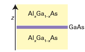
Figure 25.21 An (AlxGa1-xAs) -(GaAs) -(AlxGa1-xAs) quantum well; the thickness of the GaAs layer is on the nanoscale.
 الاكثر قراءة في مواضيع عامة في الكيمياء العضوية
 اخر الاخبار
اخبار العتبة العباسية المقدسة


